Scaling Down, Powering Up
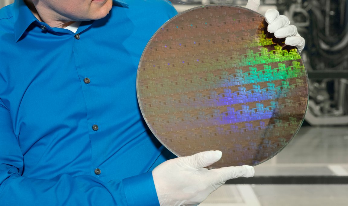
In partnership with GlobalFoundries and Samsung, IBM has unveiled the world’s first 5nm silicon chip. The chip is notable in that it is smaller than previous versions yet more dense and powerful, therefore offering higher performance. It’s also the first practical application of extreme ultraviolet (EUV) lithography and horizontal gate-all-around (GAA) field effect transistors (FETs).
Tri-gate finFETs, now used in most chip designs sized at 22nm and below, will probably be unsuitable at around 7nm. In contrast, GAAFETs — particularly in tandem with EUV — could work all the way down to 3nm. Below that size, no one yet knows what will function properly. FinFETs originally solved the volume issues older 2D transistors faced because they are 3D, increasing the volume of silicon atoms which can carry electricity by protruding from the substrate. GAAFETs can revert back into 2Ds using stackable silicon nanowires.

More Power, Less Space
According to IBM, “the new 5nm tech offers a 40 percent performance boost at the same power, or a 75 percent drop in power consumption at the same performance.” Density is also significantly improved: IBM states that it can now fit up to 30 billion transistors onto a chip 50-square-millimeters across —about the size of a fingernail. In the past, a similarly sized chip would hold 20 billion transistors at most.
As this technology continues to shrink, we will be able to fit more of it into less space. This will mean computers and other devices can become more powerful, but at the same time smaller and more portable. IBM is already on the job, having pointed out that GAAFETs are ripe for scaling down even further.