
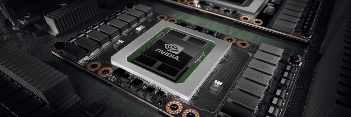
Tesla P100
Nvidia made a big splash during its keynote at the GPUTech conference in San Jose, California, when CEO Jen-Hsun Huang announced the Tesla P100, a new chip with 15 billion transistors designed for deep-learning computing.
Huang said that developing chips for deep-learning AI has now become Nvidia’s fastest growing business.
Previously, Nvidia had released two deep-learning chips, the Tesla M4 and the Tesla M40. Both chips sold out quickly, prompting the company to send the Tesla P100 into volume production. “This is the largest FinFET chip that has ever been done,” says Huang. FinFET refers to “Fin Field Effect Transistor,” a type of transistor whose non-planar design allows more computing power to be crammed into smaller spaces.
“We decided to go all-in on A.I.”

A New Focus
The Tesla P100 represents a large departure for Nvidia, a company that has focused almost solely on developing chips for workstations and gaming rigs. With the P100, Nvidia is setting their sights on data centers and deep-learning technology.
This is a huge risk as it involves the development of many other things, like a new architecture, new interconnect, and new process, all of which went into the creation of the Tesla P100.
“Our strategy is to accelerate deep learning everywhere,” said Huang.